


Description
This 3.3 V boost (step-up) voltage regulator generates higher output voltages from input voltages as low as 0.5 V, and it also automatically switches to a linear down-regulation mode when the input voltage exceeds the output. This makes it great for powering 3.3 V electronics projects from 1 to 3 NiMH, NiCd, or alkaline cells or from a single lithium-ion cell.
When boosting, this module acts as a switching regulator (also called switched-mode power supplies (SMPS) or DC-to-DC converters) and has a typical efficiency between 65% to 85%. The available output current is a function of the input voltage, output voltage, and efficiency (see Typical Efficiency and Output Current section below), but the input current can typically be as high as 1.2 A. This regulator is also available with a fixed 5 V output, and very similar 3.3V, 5V, and adjustable-output versions are available with a true shutdown option that turns off power to the load.
The regulator?s thermal shutdown engages at around 140°C and helps prevent damage from overheating, but it does not have short-circuit or reverse-voltage protection.
Features
- Input voltage: 0.5 V to 5.5 V
- Fixed 3.3 V output with 4% accuracy
- Automatic linear down-regulation when the input voltage is greater than the output voltage
- 1.2 A switch allows for input currents up to 1.2 A
- Good efficiency at light load: <1 mA typical no-load quiescent current, though it can exceed 1 mA for very low input voltages
- Integrated over-temperature shutoff
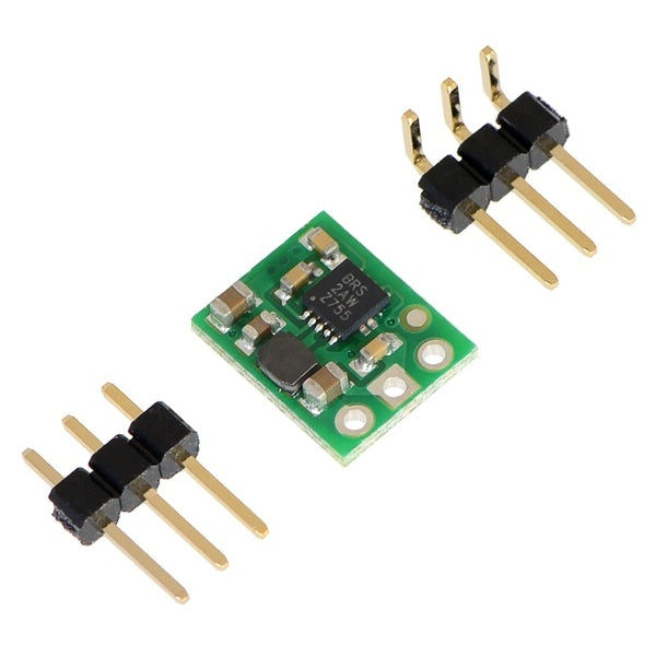
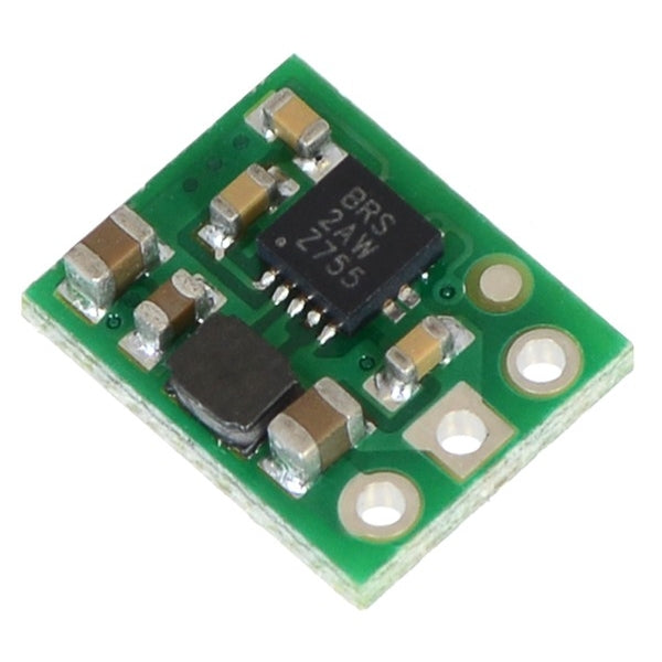
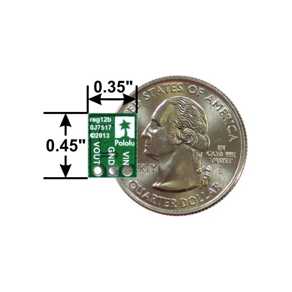
- Small size: 0.35? × 0.45?; × 0.1? (9 × 11.5 × 2.5 mm)
Using the Regulator
Connections
The boost regulator has three connections: input voltage (VIN), ground (GND), and output voltage (VOUT).
The input voltage, VIN, must be at least 0.5 V for the regulator to turn on. However, once the regulator is on, the input voltage can drop as low as 0.3 V and the 3.3 V output voltage will be maintained on VOUT. Unlike standard boost regulators, this regulator has an additional linear down-regulation mode that allows it to convert input voltages as high as 5.5 V down to 3.3 V for small to moderate sized loads. When the input voltage exceeds 3.3 V, the regulator automatically switches to this down-regulation mode. The input voltage should not exceed 5.5 V. Please be wary of destructive LC spikes that might cause the input voltage to surpass 5.5 V (see below for more information).
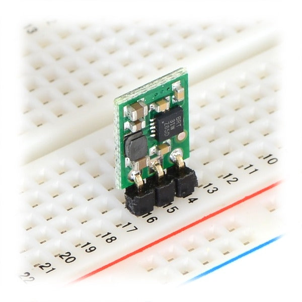
The three connections are labeled on the back side of the PCB, and they are arranged with a 0.1? spacing along the edge of the board for compatibility with solderless breadboards, connectors, and other prototyping arrangements that use a 0.1? grid. You can solder wires directly to the board or solder in either the 3×1 straight male header strip or the 3×1 right-angle male header strip that is included.

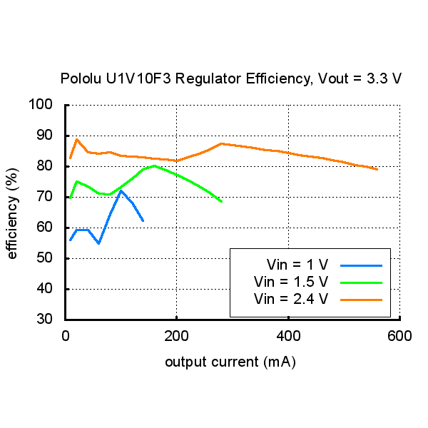
Typical Efficiency and Output Current
The efficiency of a voltage regulator, defined as (Power out)/(Power in), is an important measure of its performance, especially when battery life or heat are concerns. As shown in the graphs below, this switching regulator typically has an efficiency of 65 to 85%.
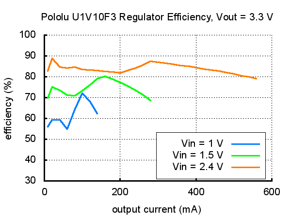
The maximum achievable output current is approximately proportional to the ratio of the input voltage to the output voltage. If the input current exceeds the switch current limit (typically somewhere between 1.2 and 1.5 A), the output voltage will begin to drop. Additionally, the maximum output current can depend on other factors, including the ambient temperature, air flow, and heat sinking.
LC Voltage Spikes
When connecting voltage to electronic circuits, the initial rush of current can cause damaging voltage spikes that are much higher than the input voltage. In our tests with typical power leads (~30? test clips), input voltages above 4.5 V caused voltage spikes that could potentially damage the regulator. You can suppress such spikes by soldering a 33 ?F or larger electrolytic capacitor close to the regulator between VIN and GND.
More information about LC spikes can be found in our application note, Understanding Destructive LC Voltage Spikes.
Specifications:
Dimensions
- Size: 0.35? × 0.45? × 0.1?1
- Weight: 0.4 g1
General specifications
- Minimum operating voltage: 0.5 V
- Maximum operating voltage: 5.5 V
- Maximum input current: 1.2 A2
- Output voltage: 3.3 V
- Reverse voltage protection?: N
- Maximum quiescent current: 1 mA3
Notes:
- 1. Without included optional headers.
- 2. Regulator may overheat at lower input currents when VIN is much lower than VOUT. Available output current is a function of VIN, VOUT, and the regulator efficiency.
- 3. The highest quiescent currents occur at very low input voltages; for most of the input voltage range, the quiescent current is well below 1 mA.
Encrypted payment
Your payment information is processed securely. We do not store credit card details nor have access to your credit card information.
Additional information
Customs Tariff Number:
Country of origin:
This depends on where you are located. After the order is handed over to UPS, the delivery time in Germany is about 2-3 days, within Europe about 1 week.
We ship our orders with UPS (United Parcel Service).
If we still haven't answered your question, you can contact us below and we will get back to you as soon as possible.
You might also like
Last viewed
