
Beschreibung
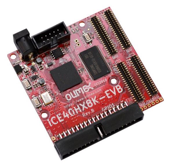
iCE40HX8K-EVB is low cost development board for iCE40 FPGA family from Lattice Semiconductor.
The interesting part about this family of FPGAs is that there is a completely free and open source development tool available.
Using this free tool you can compile Verilog designs and upload them to the FPGA. More inforomation on the link in Software section.
iCE40HX8K-EVB has 34 pin bus connector which allows the easy hardware expansion of the board with additional modules like: iCE40-ADC with 100Mhz ADC; iCE40-DAC with 100Mhz DAC; iCE40-IO with VGA, PS2 and IrDA transciever; MOD-DIO with logic analyzer level shifter with programmable 1.5-5.5V threshold. Up to 4 x ADC and 4 x DAC expansion modules can be connected on same bus (if you use iCE40-IO on the same bus then only up to 2 x ADC and 1 x DAC).
Features:
- iCE40HX8K-CT256 FPGA 7680 Logic cells, 960 LABs, 128 K embedded RAM bits
- 512KB SRAM organized as 256Kx16bit 10ns
- 2MB Serial Flash
- 2 user status LEDs
- Programming successful status LED
- 2 user buttons
- Reset button
- Power jack for 5V DC external power supply
- PGM connector (all signals at PGM1 @ 3.3V DC)
- 34 pin connector bus
- 4 x 40 pin connectors for GPIOs
- 100 Mhz oscillator
- Power supply DCDC regulators
- Power supply status LED
- Dimentions: 65x67mm
Verschlüsselte Zahlung
Ihre Zahlungsinformationen werden sicher verarbeitet. Wir speichern keine Kreditkartendaten und haben auch keinen Zugang zu Ihren Kreditkartendaten.
Zusätzliche Informationen
Zolltarifnummer:
Herkunftsland:
Das hängt davon da, wo Sie sich befinden. Nach Übergabe der Bestellung an UPS beträgt die Lieferzeit in Deutschland ca. 2-3 Tage, innerhalb Europas ca. 1 Woche.
Wir versenden unsere Artikel mit unserem Versandpartner UPS.
Wenn wir Ihre Frage noch nicht beantwortet haben, können Sie uns kontaktieren, und wir werden uns so schnell wie möglich bei Ihnen melden.
Könnte Ihnen auch gefallen
Zuletzt angesehen
