


Beschreibung
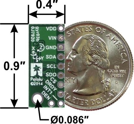
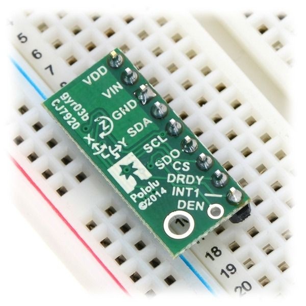
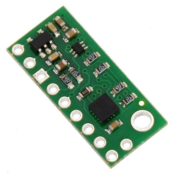
This board is a compact (0.4? × 0.9?) breakout board for ST?s L3GD20H three-axis digital-output gyroscope; we therefore recommend careful reading of the L3GD20H datasheet (3MB pdf) before using this product. The L3GD20H is a great IC, but its small, leadless, LGA package makes it difficult for the typical student or hobbyist to use. It also operates at voltages below 3.6 V, which can make interfacing difficult for microcontrollers operating at 5 V. This carrier board addresses these issues by incorporating additional electronics, including a 3.3 V voltage regulator and level-shifting circuits, while keeping the overall size as compact as possible. The board ships fully populated with its SMD components, including the L3GD20H, as shown in the product picture.
The L3GD20H has many improvements over the older L3GD20, including better accuracy and stability, lower power consumption, and a much shorter start-up time, all in a smaller package that allows the overall carrier board to be smaller. The L3GD20H also offers a wider range of user-selectable output data rates, with lower frequencies available that are more appropriate for human gesture detection, and it features a data enable (DEN) pin that allows readings to be synchronized with external triggers. While the L3GD20H carrier is not a direct drop-in replacement for the L3GD20 carrier due to differences in the pinout and sensor orientation, it should still be usable as a replacement with the appropriate wiring changes, and since the two ICs share the same register structure and I²C device address, code written for one should be easily portable to the other.
The L3GD20H has many configurable options, including three selectable angular rate sensitivities, seven selectable output data rates, seven different embedded FIFO modes for buffering output data, and a programmable external interrupt signal. The three angular velocity readings are available through a digital interface, which can be configured to operate in either I²C or SPI mode.
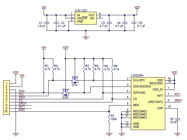
The carrier board includes a low-dropout linear voltage regulator that provides the 3.3 V required by the L3GD20H, which allows the sensor to be powered from 2.5 V to 5.5 V. The regulator output is available on the VDD pin and can supply almost 150 mA to external devices. The breakout board also includes a circuit that shifts the two I²C lines (or SPI clock and data-in lines) to the same logic voltage level as the supplied VIN, making it simple to interface the board with 5 V systems, and the board?s 0.1? pin spacing makes it easy to use with standard solderless breadboards and 0.1? perfboards.
For sensor fusion applications, our MinIMU-9 v2 and AltIMU-10 inertial measurement units combine the older L3GD20 with a LSM303DLHC 3-axis accelerometer and magnetometer on a single board, providing nine independent readings that can be used to calculate an absolute orientation. The AltIMU-10 also includes an LPS331AP pressure sensor that can be used to calculate altitude.
Specifications
- Dimensions: 0.4? × 0.9? × 0.1? (13 × 23 × 3 mm)
- Weight without header pins: 0.7 g (0.03 oz)
- Operating voltage: 2.5 V to 5.5 V
- Supply current: ~6 mA
- Output format (I²C/SPI): one 16-bit reading per axis
- Sensitivity range (configurable): ±245°/s, ±500°/s, or ±2000°/s
Included components
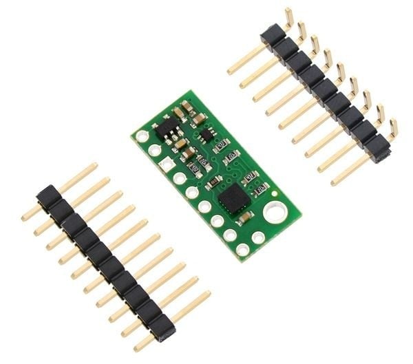
A 10×1 strip of 0.1? straight header pins and a 9×1 strip of 0.1? right-angle header pins are included, as shown in the picture below. You can solder the header strip of your choice to the board for use with custom cables or solderless breadboards, or you can solder wires directly to the board itself for more compact installations.

The board has one mounting hole that works with #2 and M2 screws (not included).
Using the L3GD20H
Connections
Regardless of the interface being used to communicate with the L3GD20H, its VIN pin should be connected to a 2.5 V to 5.5 V source, and GND should be connected to 0 volts. (Alternatively, if you are using the gyro with a 3.3 V system, you can leave VIN disconnected and bypass the built-in regulator by connecting 3.3 V directly to VDD.)
A minimum of two logic connections are necessary to use the L3GD20H in I²C mode (this is the default mode): SCL and SDA. These should be connected to an I²C bus operating at the same logic level as VIN. These pins are connected to built-in level-shifters that make them safe to use at voltages over 3.3 V.
To use the L3GD20H in SPI mode, four logic connections are typically used: SPC, SDI, SDO, and CS. These should be connected to an SPI bus operating at the same logic level as VIN. The SPI interface operates in 4-wire mode by default, with SDI and SDO on separate pins, but it can be configured to use 3-wire mode so that SDO shares a pin with SDI.


L3GD20H 3-axis gyro carrier with voltage regulator, L3GD20H 3-axis gyro carrier with
labeled top view. voltage regulator in a breadboard
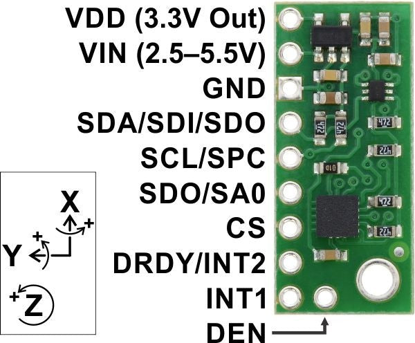
Pinout
labeled top view. voltage regulator in a breadboard
Pinout
- VIN: This is the main power supply connection, and it should be powered at 2.5 V to 5.5 V. The SCL/SPC and SDA/SDI level shifters pull the I²C and SPI bus high bits up to this level.
- GND: The ground (0 V) connection for your power supply. Your I²C or SPI control source must also share a common ground with this board.
- VDD: Regulated 3.3 V output. Almost 150 mA is available to power external components. (If you want to bypass the internal regulator, you can instead use this pin as a 3.3 V input with VIN disconnected.)
- SCL/SPC: Level-shifted I²C/SPI clock line: HIGH is VIN, LOW is 0 V
- SDA/SDI: Level-shifted I²C data line and SPI data-in line (also doubles as SDO in 3-wire mode): HIGH is VIN, LOW is 0 V
- SDO SPI: data-out line in 4-wire mode: HIGH is VDD, LOW is 0 V. Also used as a 3.3V-logic-level input to determine I²C slave address (see below). This pin is not level-shifted and is not 5V-tolerant.
- CS SPI: enable (chip select). Pulled up to VDD to enable I²C communication by default; drive low to begin SPI communication.
- DRDY/INT2: Data ready indicator, a 3.3V-logic-level output. HIGH (3.3 V) indicates angular rate data can be read. Can also be configured as a FIFO interrupt. This output is not level-shifted.
- INT1: Programmable interrupt, a 3.3V-logic-level output. This output is not level-shifted.
- DEN: Data enable trigger, a 3.3V-logic-level input. This input is not level-shifted and is not 5V-tolerant.
Schematic Diagram

The above schematic shows the additional components the carrier board incorporates to make the L3GD20H easier to use, including the voltage regulator that allows the board to be powered from a 2.5 V to 5.5 V supply and the level-shifter circuit that allows for I²C and SPI communication at the same logic voltage level as VIN. This schematic is also available as a downloadable PDF (174k PDF).
I²C Communication
With the CS pin in its default state (pulled up to VDD), the L3GD20H can be configured and its angular velocity readings can be queried through the I²C bus. Level shifters on the I²C clock (SCL) and data (SDA) lines enable I²C communication with microcontrollers operating at the same voltage as VIN (2.5 V to 5.5 V). A detailed explanation of the I²C interface on the L3GD20H can be found in its datasheet (3MB pdf), and more detailed information about I²C in general can be found in NXP?s I²C-bus specification (371k pdf).
In I²C mode, the gyro?s 7-bit slave address has its least significant bit (LSb) determined by the voltage on the SDO pin. The carrier board pulls SDO to VDD through a 4.7 k? resistor, making the LSb 1 and setting the slave address to 1101011b by default (this is the same slave address as the L3GD20). If the gyro?s selected slave address happens to conflict with some other device on your I²C bus, you can drive SDO low to set the LSb to 0.
In our tests of the board, we were able to communicate with the chip at clock frequencies up to 400 kHz; higher frequencies might work but were not tested.
SPI Communication
To communicate with the L3GD20H in SPI mode, the CS pin (which the board pulls to VDD through a 4.7 k? resistor) must be driven low before the start of an SPI command and allowed to return high after the end of the command. Level shifters on the SPI clock (SPC) and data in (SDI) lines enable SPI communication with microcontrollers operating at the same voltage as VIN (2.5 V to 5.5 V).
In the default 4-wire mode, the gyro transmits data to the SPI master on a dedicated data out (SDO) line. If the SPI interface is configured to use 3-wire mode instead, the SDI line doubles as SDO and is driven by the L3GD20H when it transmits data to the master. A detailed explanation of the SPI interface on the L3GD20H can be found in its datasheet (3MB pdf).
Sample Code
We have written a basic Arduino library for the L3G that makes it easy to interface this sensor with an Arduino. The library makes it simple to configure the L3GD20H and read the raw gyro data through I²C.
Protocol Hints
The datasheet provides all the information you need to use this sensor, but picking out the important details can take some time. Here are some pointers for communicating with and configuring the L3GD20H that we hope will get you up and running a little bit faster:
- The gyro is in power down mode by default. You have to turn it on by writing the appropriate value to the CTRL1 register.
- You can read or write multiple registers in a single I²C command by asserting the most significant bit of the register address to enable address auto-increment.
- You can enable the same auto-increment feature in SPI mode by asserting the second bit (bit 1, called the MS bit in the datasheet) of an SPI command.
Specifications:
Dimensions
- Size: 0.4? × 0.9? × 0.1?1
- Weight: 0.6 g1
General specifications
- Interface: I²C, SPI2
- Minimum operating voltage: 2.5 V
- Maximum operating voltage: 5.5 V
- Axes: pitch (x), roll (y), and yaw (z)
- Measurement range: ±245, ±500, or ±2000°/s3
- Supply current: 6 mA
Notes:
- 1. Without included optional headers.
- 2. Interface controlled by CS pin.
- 3. User-configurable.
Documents:
Verschlüsselte Zahlung
Ihre Zahlungsinformationen werden sicher verarbeitet. Wir speichern keine Kreditkartendaten und haben auch keinen Zugang zu Ihren Kreditkartendaten.
Zusätzliche Informationen
Zolltarifnummer:
Herkunftsland:
Das hängt davon ab, wo Sie sich befinden. Nach Übergabe der Bestellung an UPS beträgt die Lieferzeit in Deutschland ca. 2-3 Tage, innerhalb Europas ca. 1 Woche.
Wir versenden unsere Artikel mit unserem Versandpartner UPS.
Wenn wir Ihre Frage noch nicht beantwortet haben, können Sie uns kontaktieren, und wir werden uns so schnell wie möglich bei Ihnen melden.
Könnte Ihnen auch gefallen
Zuletzt angesehen